This is high-resolution TEM (80-200 kV) with interchangeable pole-pieces. Currently fitted with analytical pole-piece (resolution is 0.23nm, +/- 30 degrees tilt). Good control of the probe size and convergence angle for EDS, convergent beam diffraction (see fig below) and nano-beam diffraction, as well as the usual TEM facilities make this a high quality analytical facility for studying a wide range of structures.
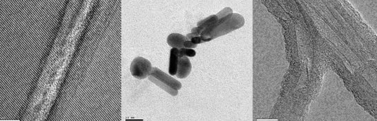
The TEM is routinely used for characterising microstructure at interfaces in ceramics, morphology and distribution of nanosize particles, lattice imaging and chemical analysis. The following images showing typical examples of a defect, gold nanoparticles, and wall thickness of carbon nanotubes.
The TEM is computer-controlled to allow users to record operation conditions, recall stored sample grid positions and perform low-dose imaging. This is useful in case for examination of biological samples that are sensitive to high energy electron beam. To record high resolution images using less energetic beams, the instrument is fitted with a Gatan Multiscan CCD camera below the viewing chamber, which makes low-intensity and high-resolution imaging possible.
Microanalysis is done on the Oxford Instruments INCA EDS 80mm X-Max detector system, which is capable of light-element (Z>5) analysis with SemiSTEM capability. A beryllium specimen holder is available to reduce or eliminate spurious x-ray signals. To reduce time due to sample exchange, a single tilt holder is available that can accommodate up to five specimens.