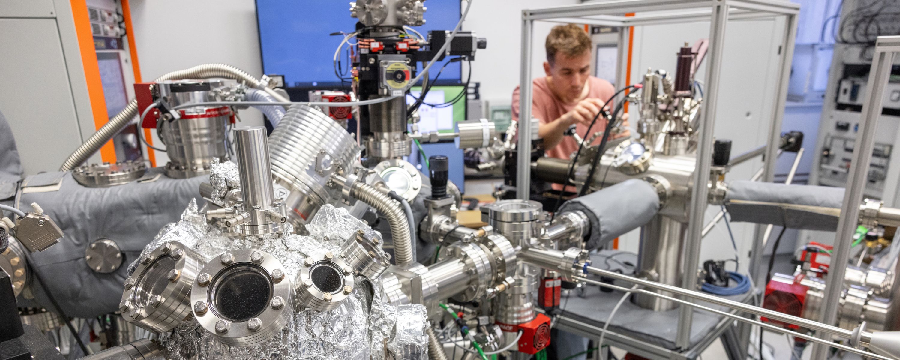
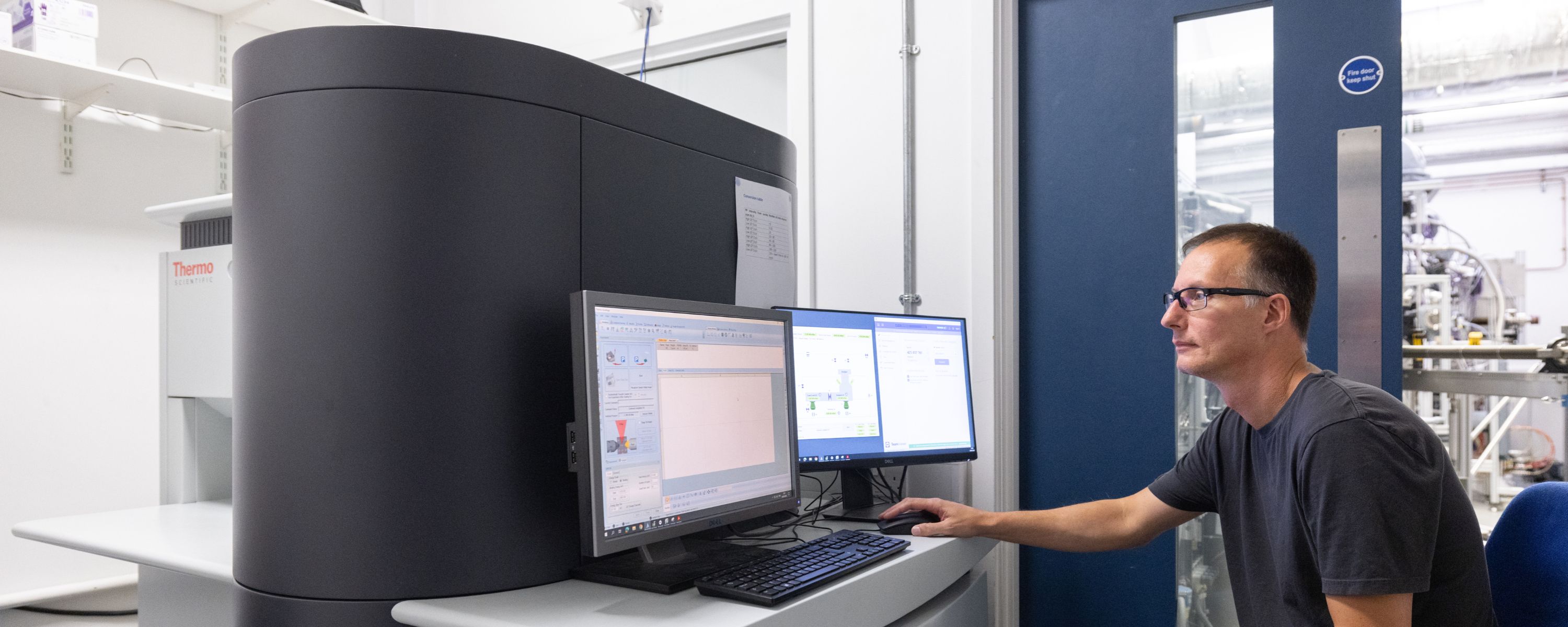
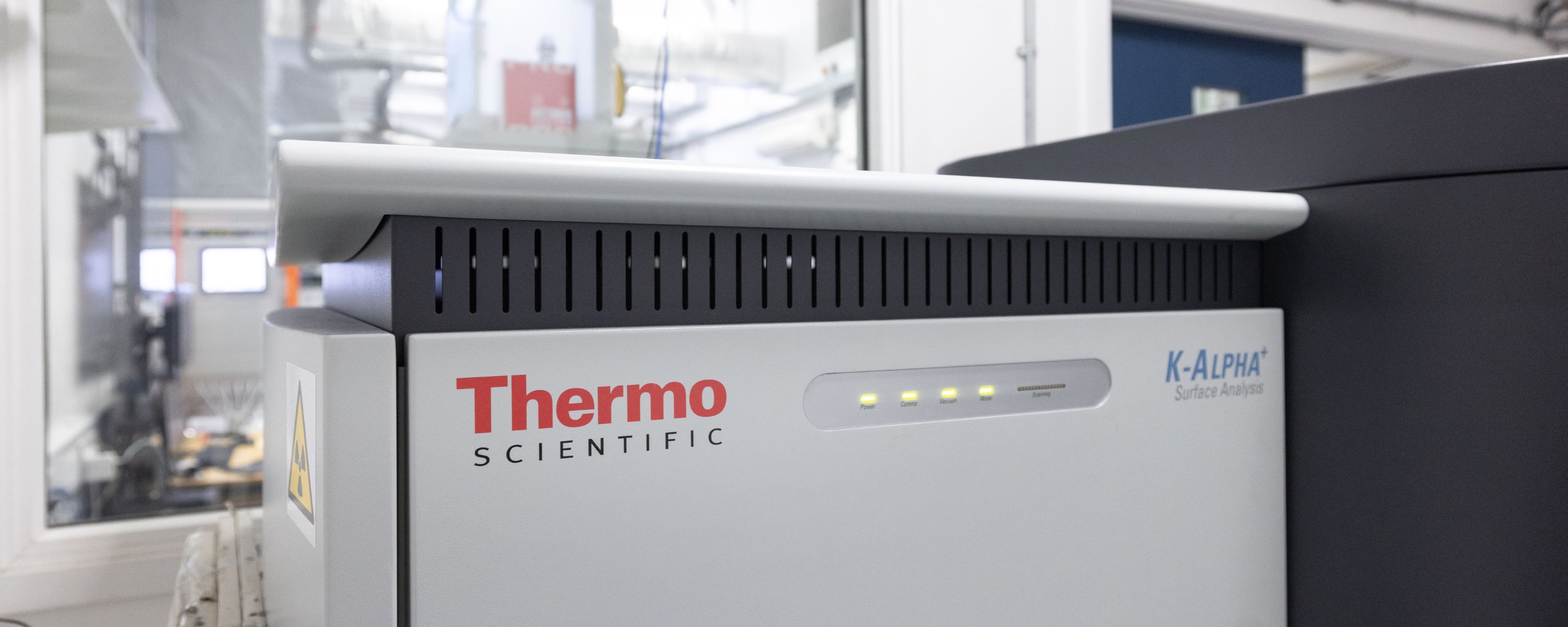
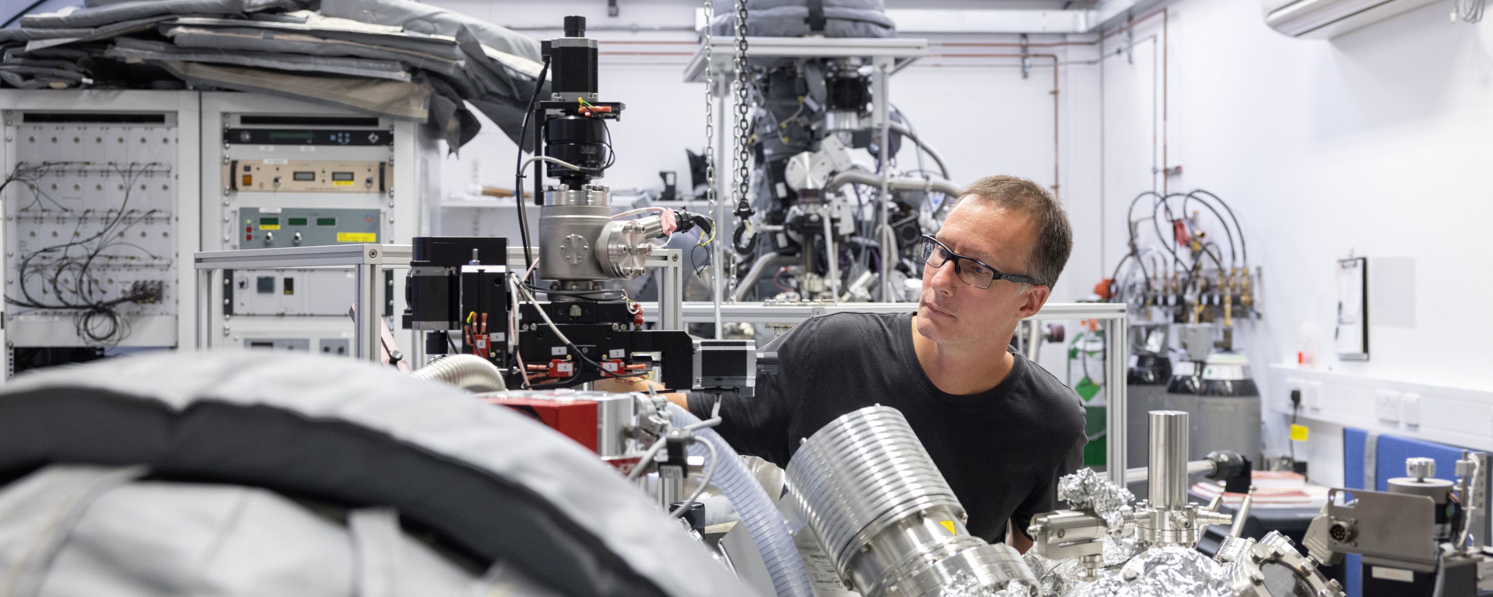
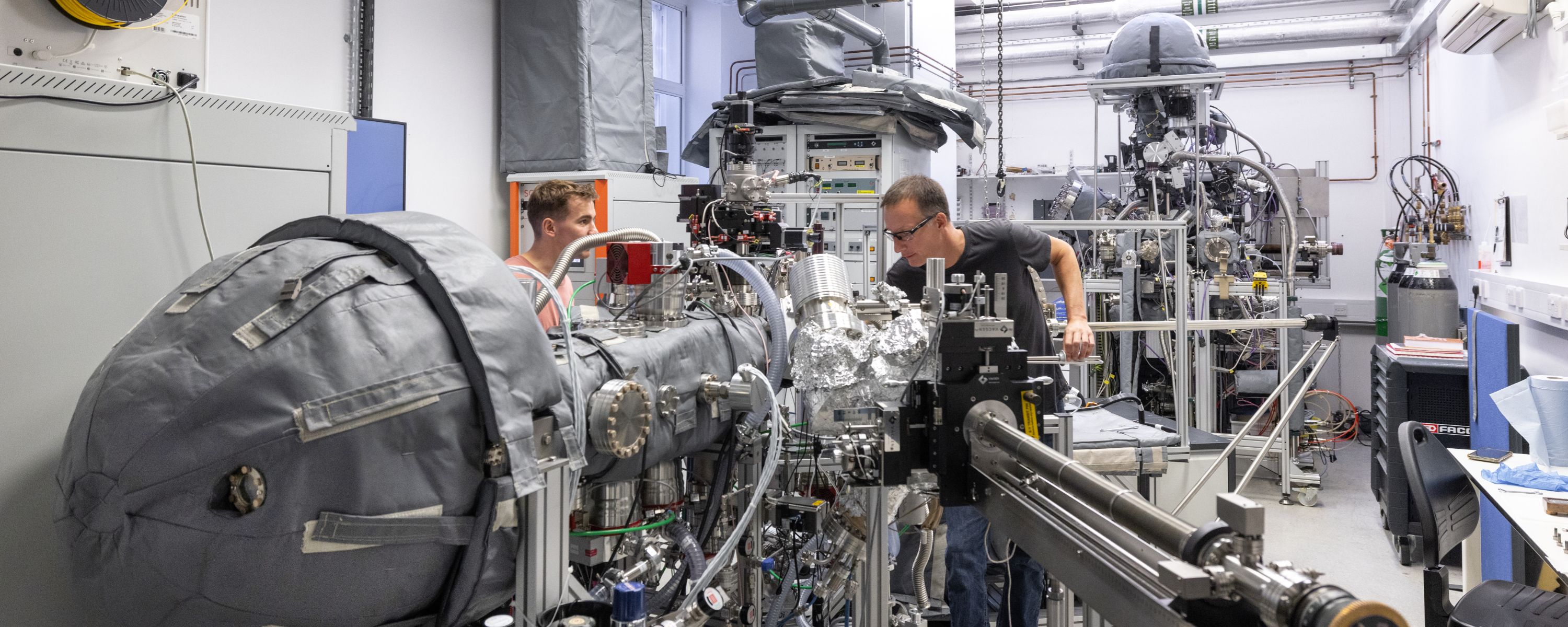
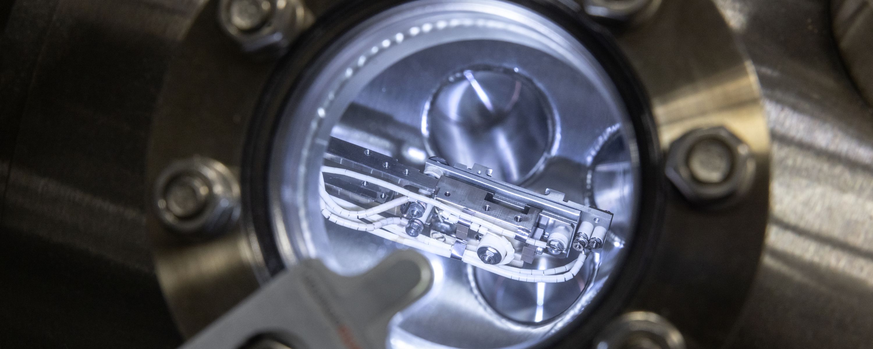
The Advanced Photoelectron Spectroscopy Laboratory (APSL) is a cutting-edge analytical facility that provides state-of-the-art surface analysis capabilities. The facility offers both high throughput XPS and near ambient pressure NAP XPS capabilities. The facility also offers UV photoelectron spectroscopy (UPS) and Low-Energy Electron Diffraction (LEED).
X-ray photoelectron spectroscopy (XPS) is a powerful technique for analysing the chemical composition and electronic state of surfaces. It provides quantitative information about the elemental composition and chemical bonding of the top few nanometers of a material's surface. The high throughput XPS is a fully automated system that allows for the rapid XPS measurement of multiple samples.
The Near Ambient Pressure X-ray Photoelectron Spectroscopy (NAP-XPS) is a cutting-edge analytical technique that allows for the in-situ measurement of surface reactions under near-ambient conditions at variable temperature. Unlike conventional XPS, which is typically performed under ultra-high vacuum conditions, NAP-XPS can be performed at pressures ranging from sub-atmospheric to several tens of millibars. This makes it possible to study surface reactions in real-world conditions that are more representative of practical applications. NAP-XPS is particularly useful for studying catalytic reactions, as it enables researchers to probe the electronic and chemical changes that occur at the surface of a catalyst during a reaction. It is also valuable for studying the surface chemistry of materials in gas-surface interactions, such as corrosion and oxidation.
UPS is an analytical technique that investigates the electronic structure of materials by irradiating them with ultraviolet photons and measuring the kinetic energy of the ejected electrons. It provides information about the work function, valence band structure, and surface composition of a material, and is often used in conjunction with XPS.
LEED is a surface-sensitive technique that studies the crystallographic structure of materials by directing a beam of low-energy electrons onto the material's surface and measuring the diffracted electrons' intensity and angular distribution. It is highly sensitive and can investigate the surface structure of materials down to the atomic scale, commonly used in materials science to investigate the crystallography of surfaces, interfaces, and thin films.
APSL help and support
-
Professor David Payne
/prod01/channel_3/media/images/people-list/DP2.jpg)
Location
Department of Materials
Royal School of Mines
2.09Support with
Full consultation to access to the NAP-XPS
-
Dr Gwilherm Kerherve
/prod01/channel_3/media/images/people-list/GK2.jpg)
Location
Department of Materials
Royal School of Mines
Lower Ground Floor, LG61Support with
Full consultation to access to the high throughput XPS
Advanced Photoelectron Spectroscopy Laboratory
