Raman Spectroscopy
Raman spectroscopy is a vibrational spectroscopy based on a molecule's polarisability. Raman spectroscopy relies on the inelastic scattering of light via a virtual excited state, leaving a molecule in an excited vibrational state. Using Raman spectroscopy we can probe the chemical structure, molecular conformation and molecular orientation of a sample. We can also use it to probe the nature of different excited states in a material.
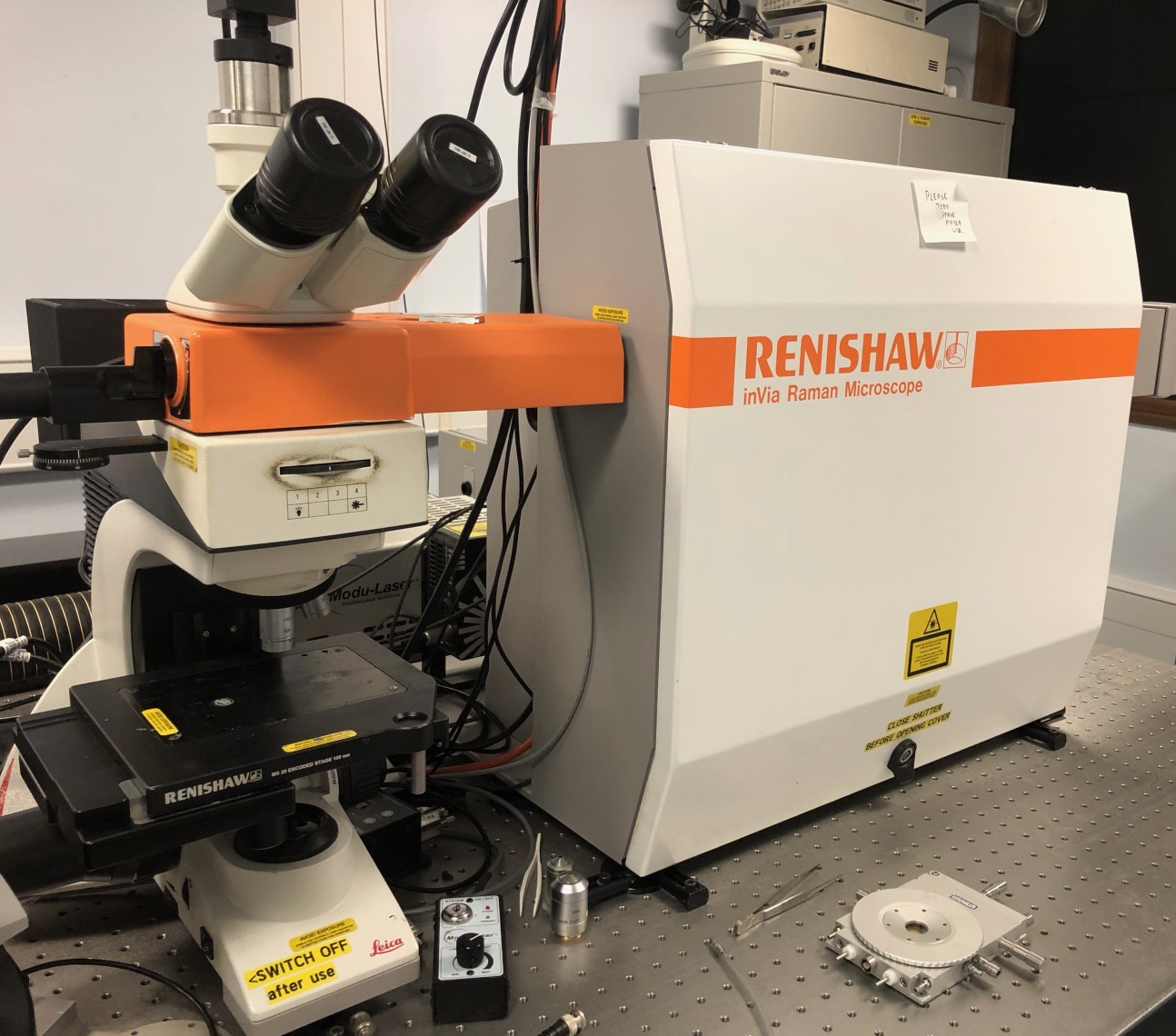
Measurements:
- 5 laser excitation wavelengths (457 - 785 nm)
- Resonant and non-resonant excitation
- Angle dependent polarisation control
- Confocal fluorescence
- Surface Enhanced Raman Spectroscopy (SERS)
- Tip Enhanced Raman Spectroscopy (TERS)
- In Situ Pressure Dependent Raman Spectroscopy
- In Situ Temperature Dependent Raman Spectroscopy (77 - 600 K)
- In Situ Device Operation
- In Situ Cyclic Voltammetry
- In Situ Electrochemical Degradation
- UV-Excitation Source
Scanning Probe Microscopy
Scanning Probe Microscopy lets us map the surface features of our thin film structures. We can generate images of our microstructures with nanometre resolution, which allows us to see the nature of different domains. Depending on the 'mode', we can image different magnetic domains, the response of a surface to charge injection or how conductive the samples are.
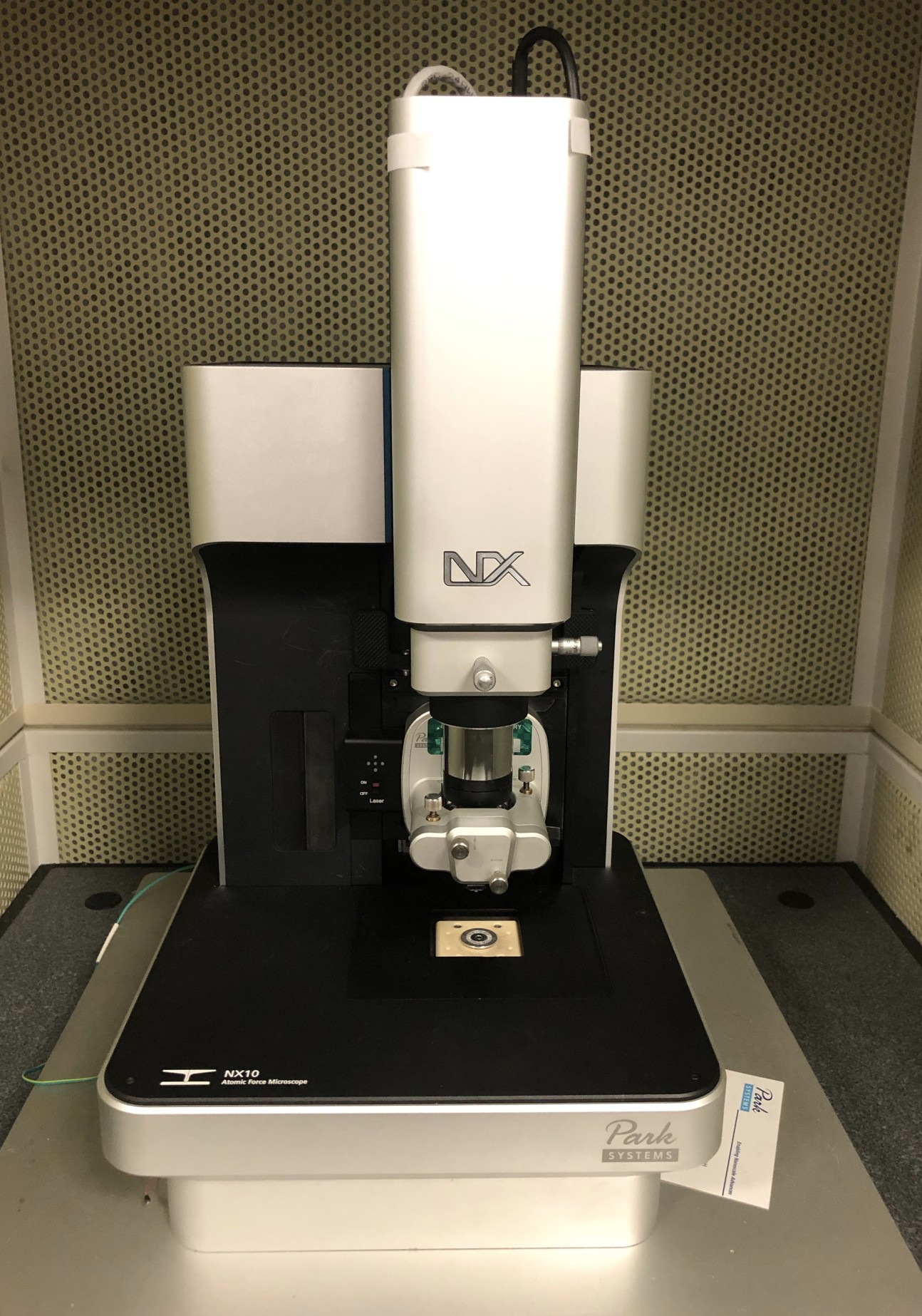
Measurements:
- Atomic Force Microscopy
- Electrostatic Force Microscopy
- Scanning Kelvin Probe Microscopy
APS-04
The APS-04 allows us to perform three different measurement techniques. Firstly the Kelvin Probe accurately measures the workfunction of metals or semiconductors by applying a backing voltage to a vibrating gold tip that sits millimetres above the sample and interpolating when the workfunctions of the two materials are aligned. Air photoelectron spectroscopy (APS) allows direct measurement of workfunction (metals) or valence band/HOMO energy levels (semiconductors) by irradiating the sample with UV light. The photoelectrons then ionise air molecules which are detected by the gold tip. Surface photovoltage spectroscopy (SPS) allows the response of a photoactive material to be obtained by irradiating the sample with different wavelengths from a quartz-tungsten-halogen (QTH) source. The photogenerated charges produce a shift in workfunction that is measured by the Kelvin probe.
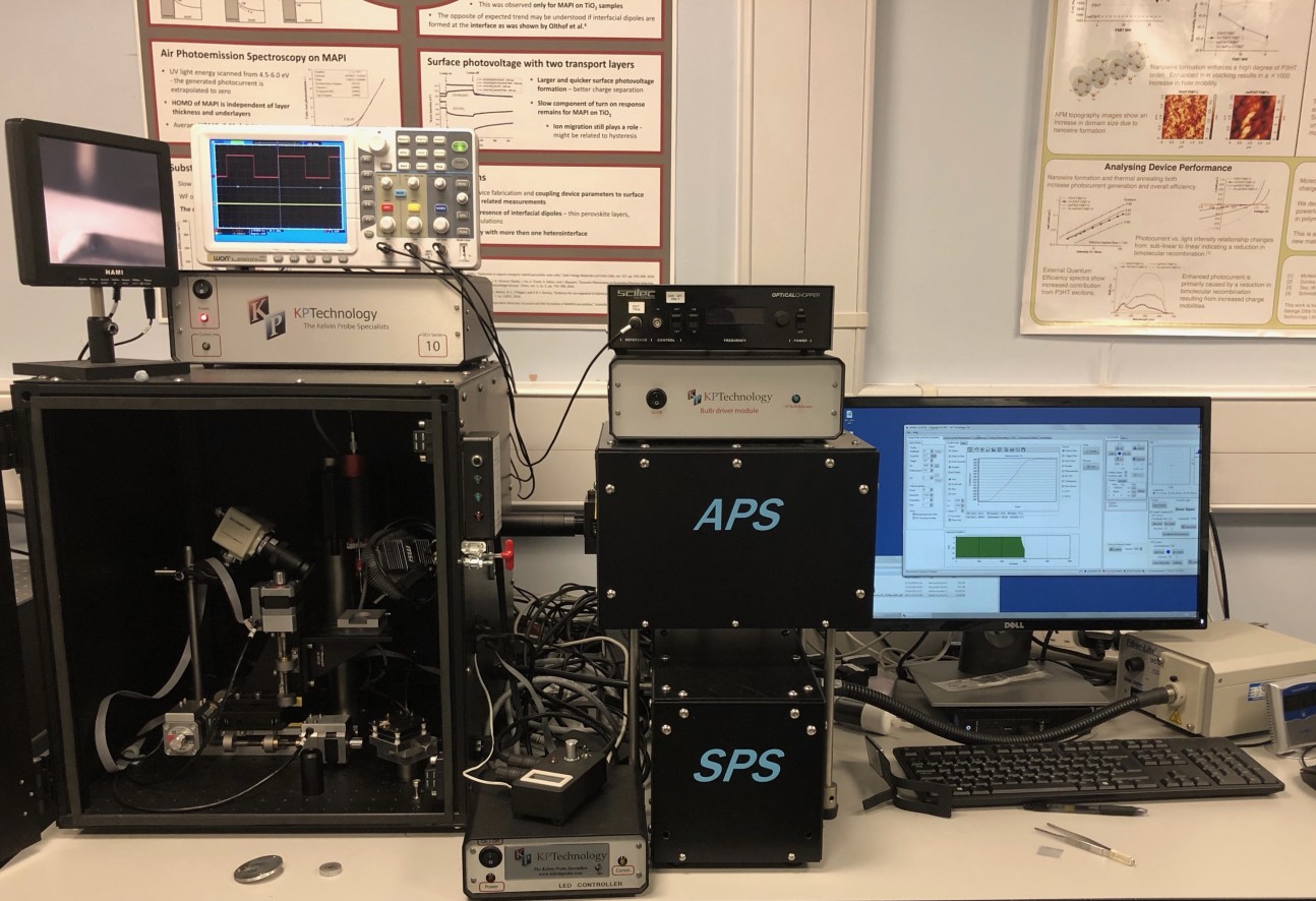
Applications in our research
-states--tojpeg_1575626033697_x4.jpg)
Interfacial energetics and tail (trap) states
We measure the energetics of organic and perovskite semiconductor materials and at their interfaces, by Ambient Photoelectron Spectroscopy (APS) and Kelvin probe. Some examples are shown below; Figure (a) dark work-function and LUMO/HOMO values of 1µm thick organic bulk heterojunction films, (b) thickness dependent Fermi-level with different contact layers, in which a large change in the work function is found below 200 nm, but almost consistent over 200nm, and (c) Tail states in different organic bulk heterojunction martials.
We have also successfully identified the origin of traps in organic BHJ PV devices, causing a significant initial drop in device efficiency. These traps were most likely caused by light-induced bond disruption or cleavage at the site of the solubilizing side chain of PC71BM electron acceptor. [Cha, H. et al, Adv. Mater., 29(33), (2017)] The light-induced chemical bond alteration and conformational twisting of the electron donor molecules were also found to be responsible for device trap formation [Luke, J. et al, Adv. Ener. Mater. 1803755 (2019)]. For the perovskite/charge injection interlayer interfaces, we found that the perovskite deposited on NiOx have lower trap density than that deposited on PEDOT:PSS, with relatively higher density of trap states preferentially formed near the interface of PEDOT:PSS and the perovskite. [Lee, S. et al., ADVANCED SCIENCE, 5(11), 10 pages. doi:10.1002/advs.201801350]
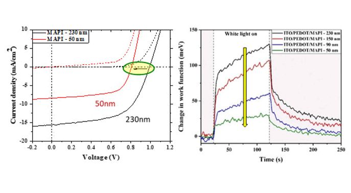
Charge accumulation leading to recombination loss
Increasing the open circuit voltage (Voc) is one of the key strategies for further improvement of the efficiency of perovskite solar cells. It requires fundamental understanding of the complex optoelectronic processes related to charge carrier generation, transport, extraction and their loss mechanisms inside a device upon illumination. We have shown the important origin of Voc losses in Perovskite based solar cells, which results from undesirable positive charge (hole) accumulation at the interface between the perovskite photoactive layer and the charge extraction layer. Using Surface Photovoltage (SPV) measurement, we show strong correlation between the thickness-dependent SPV and device performance, unravelling that the interfacial charge accumulation leads to charge carrier recombination and results in a large decrease in Voc for the PEDOT:PSS/MAPI inverted devices. In contrast, accumulated positive charges at the TiO2/MAPI interface modify interfacial energy band bending, which leads to an increase in Voc for the TiO2/MAPI conventional devices. Our results provide an important guideline for better control of interfaces in perovskite solar cells to improve device performance further.
Nanomerology 2
In-situ biosensing of metabolites
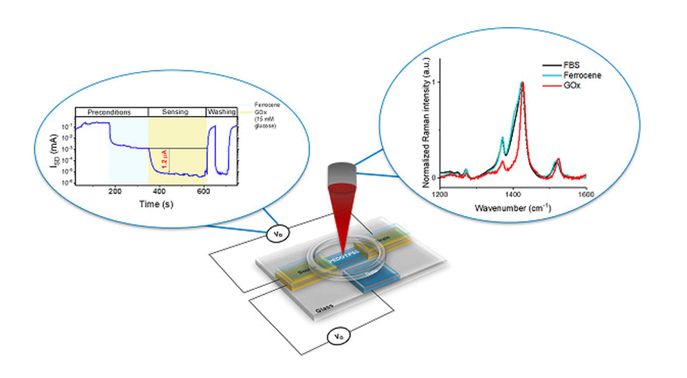
We demonstrate the use of in-situ resonance Raman spectroscopy to probe subtle molecular structural changes of PEDOT:PSS associated with its doping level. We demonstrate how such doping level changes of PEDOT:PSS can be used, for the first time, on operational organic electrochemical transistors (OECTs) for sensitive and selective metabolite sensing whilst simultaneously performing amperometric detection of the analyte. By changing the electrolyte to cell culture media, the selectivity of in-situ resonance Raman spectroscopy is emphasized as it remains unaffected by other electroactive components in the electrolyte. The application of this molecular structural probe highlights the importance of developing biosensing probes that benefit from high sensitivity of the material’s structural and electrical properties whilst being complimentary with the electronic methods of detection.
Degree of Molecular Order
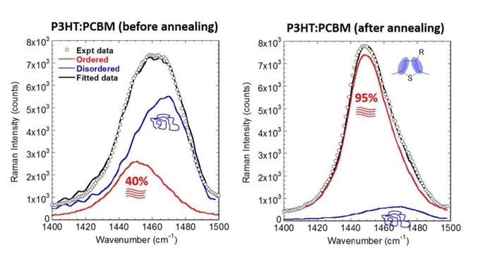
Ordering of molecules in semiconducting materials can have significant effects on their optoelectronic properties. For example, thin films of regioregular poly(3-hexylthiophene) (RR-P3HT) can exhibit a high degree of molecular order (π–π stacking of molecules). This high degree of molecular order can lead to an increase in absorption at longer wavelength and a dramatic increase in charge carrier mobility as compared to its disordered form. Understanding of this molecular order is important to clarify the structure–property relationship in thin films and to make use of these thin films as active layers in various devices.
Nanomerology 3
Natures of Electronic Transitions
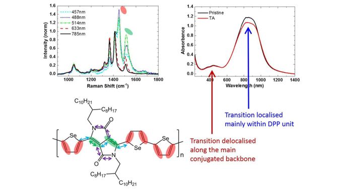
A strong resonant enhancement in the Raman scattering intensity occurs when the energy of the excitation photon matches the energy of a dipole-allowed electronic transition of the molecule. This enhancement is observed for those Raman-active vibrational normal modes which map onto the geometric distortion of the molecule accompanying the electronic transition. In order to elucidate the natures of the different electronic transitions we can use 457 and 785 nm excitations, which allow us to selectively probe the high and low energy absorption bands.
Photostability
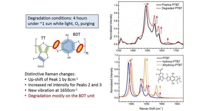
We can probe the effect of photodegradation on the molecular structure of polymer chains in order to understand how different units react with with oxygen and light at molecular level. RBy comparing experimentally observed Raman spectra to theoretical spectra obtained from Density Functional Theory (DFT) simulations of likely degradation products, we identify the nature of photo-oxidised species. This information can assist the development of analogue polymers modified to hinder or avoid that degradation process, potentially allowing the fabrication of high-efficiency long-lifetime OPV devices.
